English | हिन्दी

সিএসআইআর-কেন্দ্রীয় কাঁচ ও সেরামিক গবেষণা সংস্থা
सीएसआईआर-केंद्रीय काँच एवं सिरामिक अनुसंधान संस्थान
CSIR-Central Glass & Ceramic Research Institute
"Innovation in Ceramics and Glass for the mankind"
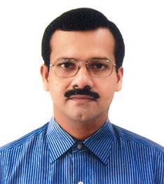
Dr. Sandip Bysakh
Senior Scientist & Head
4M Division
Contact Information:
Phone: (033) 24733496 (Ex. 3299)
FAX: +91-33-24730957
E-mail: sbysakh@cgcri.res.in
Dr. Sandip Bysakh
Joined CGCRI on 27th September 2007Professional Career
| Institution | Position | Period |
|---|---|---|
| "Joint State Key Laboratory for Materials Modification by Laser, Ion and Electron beams", Shanghai and Dalian, People's Republic of China, and Beijing Laboratory for Electron Microscopy, Chinese Academy of Sciences, People's Republic of China | Visiting Researcher | 1.4.2001 to 25.8.2001 |
| Indian Institute of Science, Bangalore | Research Associate | 01.09.2001 to 29.4.2002 |
| National Institute for Materials Science, Tsukuba, Japan | Center of Excellence Researcher | 01.05.2002 - 31.03.2004 |
| Defence Metallurgical Research Laboratory, Hyderabad | Scientist C | 12.07.2004 - 25.09.2007 |
| Central Glass & Ceramic Research Institute, Kolkata | Scientist E1 | 27.09.2007 - till date |
Education
| Degree | Discipline | University; Year |
|---|---|---|
| B.Sc. (Tech.) | Ceramic Technology | University of Calcutta |
| M.Sc (Engg.) | Metallurgy | IISc, Bangalore |
| Ph.D. | Metallurgy | IISc, Bangalore |
Patents filed / Granted
Summary: 1 (Japan,applied)
- “The method of processing materials to the nano- meter order” Shimojo Masayuki, Sandip Bysakh and Furuya Kazuo
Application number patent application 2004-75350, application day 2004.3.16
- Visiting Scientist Fellowship during April-August, 2001, State Key Laboratories for Materials Modification by Laser, Ion and Electron Beam, Shanghai and Dalian, China.
- Post Doctoral Fellow during May 2002 – April 2004 in National Institute for Materials Science, Tsukuba, JAPAN.
Research Interest
Analytical and High-Resolution Transmission Electron Microscopy (AEM & HRTEM) of materials, Nanostructured Thin Films by Pulsed Laser Ablation and RF Magnetron Sputtering, Laser Materials Processing, Non-equilibrium processing of materials, Atomic Force Microscopy of thin films.
Landmark Research Contribution
Development of pulsed laser deposition technique for deposition of thin films of advanced materials, intermetallic thin films, Development of PZT thin films for sensor application in structural health monitoring.
Selected Publications
Publications: Summary: in SCI Journal Papers = 47; in Conference Procedings = 02;
Selected papers (5):
Selected papers (5):
- “Role of TiO2 seed layer thickness on the nanostructure evolution and phase transformation behavior of sputtered PZT thin films during post-deposition air-annealing”, Ankita Bose, Monjoy Sreemany and Sandip Bysakh. ‘Journal of the American Ceramic Society’, 2011, Volume 94, 4066 – 4077.
- “Formation of amorphous xenon nanoclusters and microstructure evolution in pulsed laser deposited Ti62.5Si37.5 thin films during Xe ion irradiation”, S. Bysakh, K. Mitsuishi, M. Song, K. Furuya and K. Chattopadhyay. ‘Journal of Materials Research’, 2011, volume 26, 62 – 69.
- “Mechanisms of nano-hole drilling due to nano-probe intense electron beam irradiation on a stainless steel” S. Bysakh, M. Shimojo, K. Mitsuishi and K. Furuya ?Journal of Vacuum Science and Technology B, 2004, volume 22, 2620 – 2627.
- “A Study of Nanostructures of Thin Films in B-C-N System Produced by Pulsed Laser Deposition (PLD) and Nitrogen Ion-Beam Assisted PLD” S. Bysakh, K. Chattopadhyay, L. H. Hao, J. D. Wu, C. Dong, Y. Q. Wang, X. F. Duan and K. H. Kuo, Journal of Materials Research, 2004, volume 19, pages 759 – 767.
- “Characterization of Microstructure in Laser Surface Alloyed Layers of Aluminium on Nickel” S. Bysakh, S. K. Mitra, G. Phanikumar, J. Majumder, P. Dutta and K. Chattopadhyay, Metallurgical and Materials Transactions A?, 2003, volume 34A, pages 2621 – 2631.
Last Updated on February 28, 2025
