


English | हिन्दी
সিএসআইআর-কেন্দ্রীয় কাঁচ ও সেরামিক গবেষণা সংস্থা
सीएसआईआर-केंद्रीय काँच एवं सिरामिक अनुसंधान संस्थान
CSIR-Central Glass & Ceramic Research Institute
"Innovation in Ceramics and Glass for mankind"


Dr. Prabir Pal
Scientist-F
Multiscale Microstructure and Mechanics of Materials (4M) Division / XPS
Contact Information:
Tel.: +91-33-2322-3334
Mob: +91 9625082087
Fax: +91-33-2473-0957
E-mail: prabir.cgcri@csir.res.in
For more details click here: https://sites.google.com/site/prabirphy/
http://orcid.org/0000-0002-7356-2587
Dr. Prabir Pal
Dr. Pal joined CSIR-CGCRI on June 03, 2019Professional experience:
|
Position |
Lab/University |
Duration From |
Duration To |
Research field |
|
Scientist F |
CSIR-Central Glass and Ceramic Research Institute |
Feb-2024 |
as of now |
2D-and nano-materials, thin films for sensor applications, 2D CDW materials |
|
Principal Scientist |
CSIR-Central Glass and Ceramic Research Institute |
June-2019 |
Jan-2024 |
Photoemission, 2D-and nano-materials, thin films for sensor applications and Energy Storage Platform on Batteries |
|
Principal Scientist |
CSIR-National Physical Laboratory |
Feb-2019 |
May-2019 |
QHR standard and 2D Physics, Photoemission, Photodectector |
|
Senior Scientist |
CSIR-National Physical Laboratory |
Feb-2015 |
Jan-2019 |
Quantum Hall Resistance (QHR) standard and 2D Physics, Photoemission, Photodectector |
|
Scientist |
CSIR-National Physical Laboratory |
Feb-2011 |
Jan-2015 |
Group III-Nitride Semiconductors, Oxide Heterostructures, Photoemission, Photodetector |
|
Postdoc, Carls Triggers fellowship |
Uppsala University, Sweden |
Feb-2009 |
Jan-2011 |
Photoemission, Strongly correlated electron systems |
|
Postdoc Fellowship |
Universität Augsburg, Germany |
August-2008 |
Jan-2009 |
Photoemission, Strongly correlated electron systems |
Education
|
Degree |
Subject |
University/Institute |
Year |
|
Ph. D. |
Condensed Matter Physics |
Homi Bhabha National Institute (HBNI), IOP Campus |
2002-2008 |
|
M. Sc |
Physics |
Kalyani University, WB |
1999-2001 |
Research Interest
- Growth, Fabrication and Measurements of optoelectronic Devices
- Oxide heterostructures
- 2-D Van charge density wave (CDW) and moiré materials
Present Activity: Our main focus on novel functional epi-layers, nanomaterials, nanostructures and devices for optoelectronics and energy applications. We also study the electronic structure of ceramics, composite materials, transition metal-oxides, oxide heterostructures and 2-dimensional layered materials by using photoelectron spectroscopy.
Presently, our main scope is on the development of ceramic separators for Li-ion/Li battery. We also study the growth, fabrication and measurements of ultra-sensitive optoelectronic photodetectors.
Recent Research and Development:
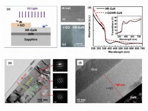
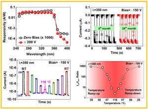
Highly resistive GaN/r-GO based photodetector for Harsh Electronics applications:
Broadband ultraviolet photodetector based on hybrid 2D/3D structure was demonstrated. The device employed a highly resistive GaN integrated with thin reduced graphene‐oxide for applications in harsh environments, working up to ±200 V bias and 116 °C with long‐term stability over 28 months without any aging effect. The device operates appreciably in both photovoltaic and photoconductive modes showing high responsivity and fast switching speed. (Advanced Optical Materials 7, 1900340, 2019)
Graphitic-C3N4/Si Binary Multifunctional Photodetector:
| A novel binary photoswitching over an ultrabroadband range was demonstrated. The device employs a hybrid 2D/3D structure based on silicon platform which opens up a possibility for the application of graphitic carbon‐nitride (g‐C3N4) nanosheets for light‐based binary communications, interconnects for optical computing and weak signal detections. This also significantly improve the performance of silicon solar cells. Covered by online scientific media (Advanced Optical Materials 6, 1800191 2018); highlighted in “Nature India” https://www.natureasia.com/en/nindia/article/10.1038/nindia.2018.76 | 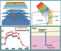 |
Self-powered Ultraviolet Photodetector:
Fabrication of high-performance photodetectors using molecular beam epitaxy grown GaN is quite challenging & extremely costly. It is thus very essential to develop simple and cost effective fabrication routes to facilitate their large-scale deployment. This works successfully demonstrated non-cleanroom fabrication of a hybrid device (r-GO/GaN) that works in self-powered mode for ultra-violet detection (Applied Physics Letters 109, 242102, 2016).
Electronic Structure of oxide heterostructures guided by electronic reconstruction revealed by Photoelectron Spectroscopy:
The electronic structure of high quality epitaxial 6 unit cells LaAl1-xCr xO3 (x = 0, 0.2, 0.4, 0.6 and 1.0) on TiO2 terminated SrTiO3 substrates were grown by pulsed laser deposition technique. We have found multiple valence states of both Ti and Cr ions, where an inverse proportionality was observed between the Ti3+ and Cr2+ valence states concentration with increasing x. The progressive increase in the concentration of Cr2+ valence states with the progressive decrease in the concentration of Ti3+ valence states as a function of x and the complete disappearance of Ti3+ states for x ³ 0.6, indicates electronic reconstruction is the most important and universal mechanism for quasi-two-dimensional electron gas in these oxides heterostructures (Physical Review B, 91, 115127, 2015).
- GATE (2002, rank 89), CSIR NET JRF 2002, JEST 2002 qualified
- Carl Tryggers Foundation Postdoctoral Fellowship, Sweden, Uppsala University, Uppsala from January, 2009 to January 2011
- Research paper Optical. Mater. 1800191, 6, (2018) highlighted in “Nature India” https://www.natureasia.com/en/nindia/article/10.1038/nindia.2018.76
- Editorial Board Member in “Advances in Materials”, Science Publishing Group
No. of Publications:
|
SCI Journals |
Conference/ proceedings |
Books chapters |
Total |
|
92 |
15 |
2 |
109 |
Recent Selected Publications (* as corresponding author)
- Insights into the Li-ion storage mechanisms in sulfur-deficient 2D VS2-x and self-intercalated V1+xS2 cathodes, S. Pal, K. Ghosh, K. Chatterjee, A. Tyagi, S. Puravankara, M. Raja, Pal*, Journal of Power Sources, 688, 240663 (2026).
- Unconventional Gas Sensing Mechanism in Phase-Separated n-Type Mixed Tungsten Oxide 2D-Nanosheets Compared against Tungsten (VI) Oxide, M. Hossain, K. Chatterjee, K. Mohanty, K. Tarafder, S. Sen, S. Kundu, E. Varrla, B. Satpati, Pal*, Small 22, e13074 (2026).
- Synthesis and characterization of phase pure barium zirconate nanoceramics by citrate acetate using the sol-gel process grown at reduced temperatures, K. Chatterjee, Pal*, Ceramics International 51, 8955 (2025).
- Charge density wave transition and unusual resistance hysteresis in vanadium disulfide (1T-VS2) microflakes, S. Pal, P. Majhi, J. Sau, S. Masanta, Pal*, M. Kumar, A. Singha, P. D. Babu, B. Ghosh, A. K. Raychaudhuri, Phys. Scr. 99, 095957, (2024).
- NO2 gas sensing performance of Ag−WO3−x thin films prepared by reactive magnetron sputtering process, M. Hossain, K. Sarkar, A. Mondal, A. Bag, P. K. Kuiri, Roopa, M. Senthil Kumar, S. Bysakh, and Pal *, Applied Physics A, 129, 866 (2023).
- Large area planar UV–Visible photodetectors using wide bandgap WO3− δ films, M. Hossain, S. Pal, S. Masanta, K. Dasgupta, T. Maity, K. Sarkar, P. Kumar, S. Bysakh, and Pal*, Optical Materials, 135, 113322 (2023).
- Solution-Processed-2D on 3D Heterojunction UV-Visible Photodetector for Low-Light Applications, G. Kumar, N. Prakash, M. Singh, A. Chakravorty, D. Kabiraj, S. P. Singh, Pal*, and S. P. Khanna, ACS Appl. Electron. Mater. 1, 1489, (2019).
- Long‐Term, High‐Voltage, and High‐Temperature Stable Dual‐Mode, Low Dark Current Broadband Ultraviolet Photodetector Based on Solution‐Cast r‐GO on MBE‐Grown Highly Resistive GaN, N. Prakash, G. Kumar, M. Singh, S. P. Singh, B. Satpati, S. P. Khanna, Pal*, Advanced Optical Materials 7, 1900340, (2019).
- Binary Multifunctional Ultrabroadband Self-Powered g-C3N4/Si Heterojunction High-Performance Photodetector, N. Prakash, G. Kumar, M. Singh, A. Barvat, Pal*, S. P. Singh, H. K. Singh and S. P. Khanna, Advanced Optical Materials 6, 1800191, (2018).
- Electronic structure of the PLD grown mixed phase MoS2/GaN interface and its thermal annealing effect, A. Barvat, N. Prakash, G. Kumar, D. K. Singh, A. Dogra, S. P. Khanna, and Pal*, Current Applied Physics 18, 170, (2018).
- Emerging photoluminescence from bilayer large-area 2D MoS2 films grown by pulsed laser deposition on different substrates, Barvat, N. Prakash, B. Satpati, S. S. Singha, G. Kumar, D. K. Singh, A. Dogra, S. P. Khanna, A. Singha, P. Pal*, Journal of Applied Physics 122, 015304 (2017).
- Photo-resistive properties of LaAl6Cr0.4O3/SrTiO3 heterostructures: a comparative study with LaAlO3/SrTiO3, Aswin V., P. Kumar, P. Pal* and A. Dogra, Optics Letters 41, 1134 (2016).
- Ultrasensitive self-powered large area planar GaN UV-photodetector using reduced graphene oxide electrodes. N. Prakash, M. Singh, G. Kumar, A. Barvat, K. Anand, P. Pal*, P. Singh and S. P. Khanna. Applied Physics Letters 109, 242102 (2016).
- Metal-to-insulator transition inLaAl1−xCrxO3/SrTiO3 oxide heterostructures guided by electronic reconstruction, P. Kumar, Pal*, A. K. Shukla, J. J. Pulikkotil, and A. Dogra, Phys. Rev. B 91, 115127 (2015).
- Chemical potential shift and gap-state formation in SrTiO3-d revealed by photoemission spectroscopy, Pal*, P. Kumar, Aswin V, A. Dogra and A. G. Joshi, Journal of Applied Physics 116, 053704 (2014).
- Photoconductivity and photo-detection response of multiferroic bismuth iron oxide. A. Anshul, H. Borkar, P. Singh, Pal, S. S. Kushvaha and A. Kumar; Applied Physics Letters 104, 132910 (2014).
- Electronic structure of the electron-doped CMR Ca86Pr0.14MnO3. M. K. Dalai, P. Pal, B. R. Sekhar, M. Merz, P. Nagel, S. Schuppler, and C. Martin, Phys. Rev. B 85, 155128 (2012).
- A simple method to produce almost perfect graphene on highly oriented pyrolytic graphite. M. J. Webb, P. Palmgren, Pal, O. Karis and H. Grennberg, Carbon 49, (2011) 3242-3249.
- Pseudogap behavior in Pr5Sr0.5MnO3: A photoemission study. P. Pal*, M. K. Dalai and I. Ulfat, Surface Science 605, 875-877 (2011).
- Atomic scale chemical fluctuation in LaSrVMoO6: A proposed halfmetallic antiferromagnet. S. Jana, V. Singh, S. D. Kaushik, C. Meneghini, Pal, R. Knut, O Karis, I. Dasgupta, V. Siruguri, S. Ray, Phys. Rev. B (Rapid Communications) 82, 180407(R) (2010).
- Pseudogap behavior of phase-separated Sm1-xCaxMnO3: A comparative photoemission study with double exchange. Pal, M. K. Dalai, R. Kundu, B. R. Sekhar and C. Martin, Phys. Rev. B. 77, 184405 (2008).
- Near Fermi Level Electronic Structure of Pr1-xSrxMnO3: Photoemission study. Pal, M. K. Dalai, R. Kundu, M. Chakraborty, B. R. Sekhar and C. Martin, Phys. Rev. B 76, 195120 (2007).
- Electronic structure of Pr67Ca0.33MnO3 near the Fermi level studied by ultraviolet photoelectron and x-ray absorption spectroscopy. M. K. Dalai, P. Pal, B. R. Sekhar, N. L. Saini, R. K. Singhal, K. B. Garg, B. Doyle, S. Nanarone, C. Martin, and F. Studer, Phys. Rev. B 74, 165119 (2006).
- Valence band electronic structure of Pr1-xSrxMnO3 from photoemission studies. Pal, M. K. Dalai, B. R. Sekhar, S. N. Jha, S. V. N. Bhaskara Rao, N. C. Das, C. Martin, and F. Studer, J. Phys. Condens. Matter 17, 2993 (2005).
Recently delivered invited talks and session chair:
[13] Delivered Invited lecture at Condensed Matter Days-2025, (CMDAYS-2025), a national level conference organized by Department of Physics, Visva-Bharati University from 29th to 30th October, 2025, (Invited) Title of talk: “Two-Dimensional (2D) Physics: Interface Electronic Structure and Optoelectronic Sensors”.
[12] Delivered Invited lecture at Department of Physics, Sidho-Kanho-Birsha University, Purulia – 723104, West Bengal, in the one-week training program on “Advanced Equipment for probing matter and radiation” from 13-19th Dec, 2022 under DST-STUTI Programme funded by DST. Title of talk: “X-ray Photoelectron Spectroscopy: Characterization Technique”
[11] Delivered Invited lecture at Department of Physics, Birla Institute of Technology, Mesra, Ranchi, India, in the high end workshop on Nanostructured Devices funded by SERB on 12-14 Dec, 2022. Title of talk: “Synthesis, characterizations and device applications of 2D materials”
[10] Delivered Special lecture at Department of Physics, Sidho-Kanho-Birsha University, Purulia – 723104, West Bengal on 25th March, 2022. Title of talk: “Photoemission and Photoconductivity Characterization of Oxide and Nitride Heterostructure Materials”
[9] Delivered 26th Institute Internal Seminar (26 IIS) on 10th March, 2022 (Thursday) at CGCRI. Title of talk: “Photoemission and Photoconductivity Characterization of Oxide and Nitride Heterostructure Materials”
[8] Delivered one invited talk in the 2nd International Conference on Ubiquitous & Emerging Concepts on Sensors & Transducers – UEMCOS2020 from 16th to 18th October 2020 in virtual mode at University of Engineering & Management, Kolkata, title: “Development of Hybrid Photodetector based on 2D and 3D GaN materials”
[7] Delivered two invited lectures in the faculty development program at Jaypee Institute of Information Technology (JIIT) – Noida, 01-06th July, 2019, organized by department of Physics and Materials Science & Engineering, JIIT, title: “Familiarization with X-ray Photoelectron Spectroscopy (XPS) method and technique”
[6] Delivered an invited talk on 16th March, 2018 at Jaypee Institute of Information Technology (JIIT) – Noida in the National Conference on Advanced Materials and Nanotechnology (AMN-2018) 15-17th March 2018, organized by department of Physics and Materials Science & Engineering, JIIT, title: “Two-Dimensional (2D)-MoS2 Layered Materials: Electronic Structure and Optoelectronic Devices”
[5] Delivered an invited talk on 27th December, 2017 at IISER-Bhopal in the National Conference on Electronic Structure (NCES-2017) Organized by TIFR, IOP and SINP, title: “Two-Dimensional (2D) MoS2 Layered Materials: Electronic Structure and Optoelectronic Devices”
[4] Delivered an invited talk on 17th March, 2017 title: “Oxide thin films and Optoelectronic Devices”, during 16-17th, 2017, LEOS (Laboratory for Electro-Optics System), ISRO, Peenya, Karnataka, Bangalore, India
[3] Delivered an invited speech on 23rd Sept, 2016 at UGC Sponsored National Level Seminar on “Characterization of Nanomaterials” Organized by Dept. of Physics, Ramananda College, Bishnupur, Bankura W.B, during September 22-23, 2016 title: “Introduction to X-ray Photoelectron spectroscopy and Photoconductivity on material characterization”
[2] Session Chair at UGC Sponsored National Level Seminar on “Characterization of Nanomaterials” Organized by Dept. of Physics, Ramananda College, Bishnupur, Bankura W.B, during September 22-23, 2016.
[1] Delivered an invited talk on 23rd Feb, 2016 title: “Interface properties of oxide heterostructures”, at Workshop on Frontiers in Condensed Matter Physics” in Feb. 22nd – 27th, 2016 at IOP, Bhubaneswar, India.
Current Projects:
- Engineering of Superstructure Orders in 2-Dimensional (2D) V(S/Se/Te)₂ Materials sponsored by Anusandhan National Research Foundation (ANRF) under ARG scheme sanction no ANRF/ARG/2025/001743/ENS from 04.06.2026 to 03.06.2029, PI
Completed Projects: Five
5. Energy Storage Platform on Batteries, sponsored by DST, Co-principal investigator (August 2019 to July 2023), Scope: Development of Ceramic Separators for Li-ion battery, Co-PI
4. Growth & Characterization of III-nitride Hetero-structures for Solid State Lighting devices, under Efficient Silicon Photovoltics with Smart Electronics and Lighting System a network project sponsored by CSIR under Technologies and Products for Solar-energy Utilization through Networks- “TAP-SUN” 2012-2017 (Team member)
3. MBE grown GaN/InxGa1-xN high efficiency multi junction Solar cell, under the project entitled Development of Advanced Materials for Next Generation Energy Efficient Devices (D-NEED) PSC0109 funded by CSIR under 12th FYP 2012-2017 (Team member)
2. Photoconductivity of novel materials – Exploiting new experimental resources, funded by CSIR-NPL, LRF (OLP 120132) 2011-2015: “Variable Temperature Steady State Photoconductivity” facility was developed in this project at CSIR-NPL (Principal Investigator)
1. Fabrication of LED Devices and Systems for Solid State Lighting (NWP-25), A supra-institutional network project sponsored by CSIR under 11th FYP 2007-2012 (Team member)
Ph. D Supervision:
- Samanta Pal, CSIR NET (Date of joining July 2020)
- Kaustuv Chatterjee, DST INSPIRE (Date of joining 1st August, 2022)
- Subhadip Sardar, UGC-NET (Date of joining 27.01.2025)
Former Member
Postdoc:
- Krishnendu Sarkar, Inspire Faculty (9th Jan, 2022 to 17th Sept, 2025), now at Universite Paris Saclay (Marie curie postdoc)
Ph. D degree awarded (AcSIR): 03
- Modassar Hossain, CSIR NET, Jadavpur University (2019-2026), Job: Teacher School (Howrah)
- Nisha Prakash, UGC-NET (2014-2020) AcSIR (CSIR-NPL) Job: Senior Scientist Position in First Solar
- Arun Barvat UGC-NET (2014-2019) AcSIR (CSIR-NPL) Postdoc
M. Tech thesis completed = 04
Openings:
Ph. D Position:
We invite applications from motivated students who are CSIR-NET INSPIRE qualified for our Ph.D. program. Candidates with a background in Physics or Chemistry are encouraged to apply. Eligible NET/ INSPIRE qualified students may contact us for further details [prabir.cgcri@csir.res.in].
Postdoctoral Research Associated Position:
We are seeking a postdoctoral researcher to join our group. Candidates interested in applying for a fellowship (such as NPDF, Inspire Faculty or others) are encouraged to reach out. Ph.D. students who are interested may contact us directly with their CV, a list of publications, and a brief overview of their past research activities.
Short Term Project: Interested students may apply for short-term projects.










Last Updated on September 29, 2026
